
Wafer Frame - Semiconductor Precision Part Manufacturer
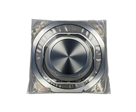
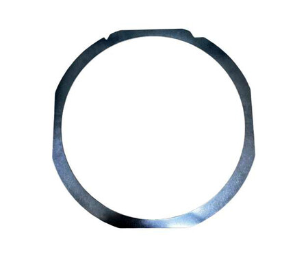
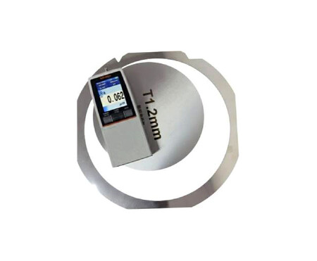
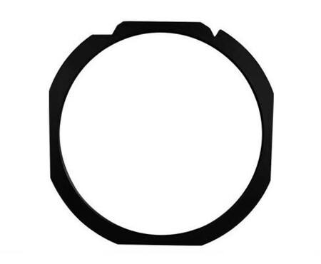
A Wafer Frame, also known as a Wafer Ring or Dicing Ring, is an essential precision carrier used in semiconductor back-end packaging and wafer dicing processes. Its primary function is to provide a stable, flat, and high-rigidity mechanical support platform during wafer back grinding, dicing, and subsequent pick-and-place operations, ensuring that wafers maintain structural integrity and positioning accuracy under high-precision and high-stress processing conditions. Each part is machined to the customer drawing in tungsten carbide, tool steel, stainless steel, precision ceramics or copper alloy, with micron-level dimensional control and metrology verification before shipment.

Wafer Frame
Wafer Ring
A Wafer Frame, also known as a Wafer Ring or Dicing Ring, is an essential precision carrier used in semiconductor back-end packaging and wafer dicing processes. Its primary function is to provide a stable, flat, and high-rigidity mechanical support platform during wafer back grinding, dicing, and subsequent pick-and-place operations, ensuring that wafers maintain structural integrity and positioning accuracy under high-precision and high-stress processing conditions.
As semiconductor manufacturing continues to advance toward thinner wafers, higher-density packaging, and greater automation, wafer frames are no longer merely handling carriers. They have become critical components that directly impact dicing accuracy, equipment stability, automation efficiency, and overall production yield.
Zhanyang specializes in the design and manufacturing of high-precision wafer frames, combining extensive semiconductor process expertise, advanced flatness control technology, and automation integration capabilities. We provide comprehensive one-stop solutions ranging from design development and material selection to mass production manufacturing, helping customers enhance process stability, improve manufacturing efficiency, and achieve higher production yields.
Wafer Frame Product Positioning
Wafer Frames are primarily used in semiconductor back-end processes for wafer holding, handling, and dicing support. Their core functions include:
● High Flatness Wafer Support
● Wafer Positioning and Retention
● Precision Dicing Process Support
● Automation Compatibility
● Clean & Stable Process Support
Based on wafer size and equipment requirements, Wafer Frames can be custom-designed with various materials, dimensions, tolerances, and structural configurations to meet the needs of different semiconductor packaging and wafer processing applications.
Key Challenges & Customer Pain Points
In high-precision semiconductor manufacturing environments, customers demand extremely high standards in flatness, dimensional accuracy, and cleanliness of Wafer Frames. Insufficient frame flatness can lead to wafer warpage, which may negatively affect dicing depth control and overall process accuracy. Inconsistent dimensional tolerances can also cause automation positioning errors, equipment jams, or machine collisions.
In addition, poor material cleanliness or inadequate surface quality may generate particles, adhesive residues, or contamination risks, affecting semiconductor yield and equipment stability. For high-volume and highly automated production lines, customers are concerned not only with the frame itself, but also with its ability to maintain long-term stability, repeatability, and cleanliness throughout production.
The Role of Wafer Frames in Semiconductor Manufacturing
Wafer Frames are widely used in:
● Wafer Back Grinding
● Wafer Dicing
● Die Sorting and Pick-and-Place Processes
● Wafer Transportation, Storage, and Shipping
● Automation Handling and Process Equipment Integration
Their primary role is to provide a high-rigidity, high-flatness, and standardized support platform, enabling wafers to be processed and transported safely and consistently across various automated systems and precision manufacturing processes.
Impact of Product Quality on Manufacturing Performance
Poor-quality Wafer Frames may result in:
● Inconsistent dicing depth causing die chipping or cracking
● Wafer movement leading to batch-level defects
● Equipment jams and unplanned downtime in automated systems
● Latent mechanical stress affecting package reliability
● Particle contamination reducing process yield
High-quality Wafer Frames help improve:
● Wafer flatness and positioning stability
● Consistency of dicing and grinding accuracy
● Process stability and long-term production capability
● Equipment utilization and automation efficiency
For advanced semiconductor and packaging applications, the flatness, rigidity, and cleanliness of Wafer Frames directly influence final product quality and equipment performance.
Customer Benefits
Implementing high-quality Wafer Frames provides customers with numerous advantages:
● Improved dicing and grinding process yield
● Reduced risk of die chipping, cracking, and latent defects
● Increased equipment utilization and manufacturing efficiency
● Lower wafer scrap rates and reduced total cost of ownership (TCO)
● Enhanced long-term production stability and product consistency
Helping customers establish a semiconductor manufacturing environment with superior stability, cleanliness, and productivity.
Zhanyang's Technical Advantages and Service Features
Zhanyang has extensive experience in semiconductor precision carriers and high-precision component manufacturing. We possess deep expertise in flatness control, material stability, and equipment integration requirements for wafer dicing, grinding, and automated handling applications.
We do not simply manufacture according to drawings. Instead, we approach every project from the perspectives of process stability and equipment efficiency, helping customers optimize structural design, material selection, and product lifespan to further improve manufacturing yield and equipment reliability.
Through high-precision CNC machining, advanced flatness control, and precision metrology capabilities, we consistently maintain strict dimensional tolerances and structural accuracy. We also offer a wide range of material options, including metals, engineering plastics, and high-performance resins, to accommodate different process environments and equipment requirements.
Additionally, we provide laser marking, barcode traceability, automation-compatible designs, and cleaning / regeneration services, enabling customers to establish a more comprehensive and efficient wafer carrier management solution. Zhanyang is a trusted technology partner in semiconductor manufacturing and automation integration.
Materials & Manufacturing Capabilities
Zhanyang offers customized Wafer Frame manufacturing using a variety of materials:
● Stainless Steel (SUS420J2, SUS316, etc.)
● Engineering Plastics (PPS, ABS, and other specialty polymers)
● Magnesium-Aluminum Alloys
Our manufacturing capabilities include:
● Precision CNC Machining
● High Flatness and High Rigidity Control
● Micron-Level Dimensional Measurement
● Surface Treatment and Clean Manufacturing Processes
● Laser Marking and Traceability Identification
● Customized Automation Equipment Integration Design
Meeting the stringent semiconductor industry requirements for dimensions, tolerances, cleanliness, and long-term production stability.
Applications
Wafer Frames are widely used in:
● Semiconductor Packaging and Testing (OSAT)
● Foundry and Backend Wafer Processing
● Memory, Logic, and Power Device Manufacturing
● Automotive and High-Reliability Semiconductor Products
● Highly Automated and Precision Semiconductor Production Lines
● Glass and Substrate Dicing Applications
Especially suitable for advanced manufacturing environments requiring high flatness, high cleanliness, and high automation compatibility.
Why Choose Zhanyang
A Wafer Frame is far more than a simple carrier—it is a critical foundation that connects wafer dicing, transportation, automation, and yield control. In highly precise and automated semiconductor manufacturing environments, even minor deviations in flatness, dimensional accuracy, or cleanliness can directly impact equipment stability and final product quality.
Zhanyang understands the semiconductor industry's stringent requirements for consistency and reliability. From material selection and manufacturing methods to quality verification, every step is driven by a commitment to superior flatness, cleanliness, and long-term production stability.
With years of experience in semiconductor carrier development, advanced precision machining capabilities, and rapid customization services, Zhanyang helps customers establish more stable and efficient wafer manufacturing environments, making us a trusted long-term technology partner in semiconductor and advanced packaging industries.
Popular Products
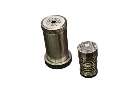
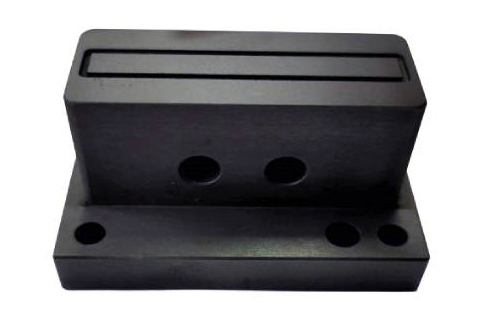

Wafer Frame| Custom Precision Manufacturing for Semiconductor Equipment
Wafer Frame is designed for semiconductor packaging and wafer-handling equipment where component geometry, machine interface and contact surfaces must match the requirements of the installed process. Zhanyang can manufacture custom fixtures from customer drawings and equipment specifications when supported by the project requirements.
Material selection and machining methods depend on factors such as operating conditions, dimensional tolerances, contact requirements and equipment compatibility. Depending on the design, available processes may include precision CNC machining, grinding, polishing, micro-hole machining and dimensional inspection, with materials selected according to the verified application requirements.

One-Stop Custom Solutions
We provide one-stop services from design and material selection to CNC precision machining, assembly, and validation.

Micron-Level Machining
Our advanced machining capabilities achieve micron-level precision, ensuring exceptional accuracy, consistency, and reliability.

Higher Yield, Lower Cost
High-quality components improve yield, boost equipment stability, reduce costs, and strengthen competitiveness.