
Bonding Head / Bond Tool - Semiconductor Precision Part Manufacturer
The Bonding Tool (Bond Head Tip) is a critical component in semiconductor packaging processes and is widely used in high-precision advanced packaging applications such as Die Bonding, Thermo-Compression Bonding (TCB), Flip Chip, and Hybrid Bonding. Its primary function is to accurately and consistently transfer pressure and thermal energy to the die or package surface during the bonding process, ensuring superior bond quality, positioning accuracy, and long-term product reliability. Each part is machined to the customer drawing in tungsten carbide, tool steel, stainless steel, precision ceramics or copper alloy, with micron-level dimensional control and metrology verification before shipment.

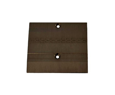
Bonding Head / Bond Tool
The Bonding Tool (Bond Head Tip) is a critical component in semiconductor packaging processes and is widely used in high-precision advanced packaging applications such as Die Bonding, Thermo-Compression Bonding (TCB), Flip Chip, and Hybrid Bonding. Its primary function is to accurately and consistently transfer pressure and thermal energy to the die or package surface during the bonding process, ensuring superior bond quality, positioning accuracy, and long-term product reliability.
As technologies such as Artificial Intelligence (AI), High-Performance Computing (HPC), High Bandwidth Memory (HBM), and advanced high-density packaging continue to evolve, the bonding tool has become far more than a simple contact component. It now plays a critical role in determining thermal transfer efficiency, bonding strength, package yield, and product lifespan.
Zhanyang specializes in the design and manufacturing of high-precision bonding tools, combining extensive semiconductor packaging expertise, micron-level machining capabilities, and advanced material integration technologies. We provide a comprehensive one-stop solution—from design development and material selection to precision manufacturing and volume production,helping customers enhance advanced packaging process stability, improve production yield, and achieve long-term manufacturing reliability.
Custom Bonding Tool Positioning
The Bonding Tool is a critical component in semiconductor packaging processes, responsible for thermal and force transfer during chip bonding. Its primary functions include:
● Precision Force Control
● Stable Thermal Transfer
● Precision Bonding of Dies and Package Structures
● Improved Yield and Reliability
● Support for Advanced Packaging Processes
To meet different packaging requirements, Bonding Tools can be customized with single-point, multi-point, matrix-pattern, or specialized micro-structured contact surfaces. Various high-performance materials with excellent thermal conductivity, high hardness, and low thermal expansion can also be selected to suit different chip types and process conditions.
Key Challenges & Customer Pain Points
In advanced semiconductor packaging and high-precision bonding applications, customers often face challenges such as uneven pressure distribution, insufficient heat transfer, and limited material durability. Poor Bonding Tool design may result in excessive localized stress, leading to die cracking, incomplete bonding, or insufficient bond strength.
Furthermore, under high-temperature and high-pressure processing conditions, materials with inadequate thermal stability may deform, wear prematurely, or experience thermal drift, reducing long-term production stability and product reliability. For advanced AI, HBM, and advanced packaging applications, customers require not only successful bonding but also consistent high precision, repeatability, and long-term process reliability.
The Role of Bonding Tools in Semiconductor Manufacturing
Bonding Tools are widely used in:
● Die Bonding
● Thermo-Compression Bonding (TCB)
● Flip Chip Packaging
● Hybrid Bonding
● Advanced Packaging and Fine-Pitch Interconnection Applications
Their primary role is to serve as the final interface for transferring heat and force, precisely applying thermal energy and pressure to dies and package structures to ensure bonding quality, alignment accuracy, and long-term product reliability.
Impact of Bonding Tool Quality on Manufacturing
Poor-quality Bonding Tools may cause:
● Die cracking or incomplete bonding due to uneven pressure
● Inconsistent heat transfer affecting soldering and bonding quality
● Surface scratches and contamination caused by wear or poor surface finish
● Reduced bonding accuracy and poor process repeatability
● Thermal drift and performance degradation during long-term production
High-quality Bonding Tools help improve:
● Uniform pressure distribution and process stability
● Thermal transfer efficiency and bonding quality
● Packaging yield and product reliability
● Long-term production stability and equipment performance
For advanced packaging and high-reliability applications, the material properties, flatness, and machining precision of Bonding Tools directly influence final product quality and packaging performance.
Customer Benefits
Implementing high-quality customized Bonding Tools provides customers with numerous advantages, including:
● Higher Die Bonding and TCB process yields
● Reduced die damage and bonding defects
● Improved bond strength and product reliability
● Enhanced equipment stability and production efficiency
● Extended tool life with lower replacement costs
● Greater competitiveness in advanced semiconductor packaging
Helping customers establish highly precise, stable, and reliable advanced packaging production lines.
Zhanyang's Technical Advantages and Service Features
Zhanyang has extensive experience in developing critical semiconductor packaging components, particularly for thermo-compression bonding, fine-pitch packaging, and precision force control applications. Beyond manufacturing Bonding Tools according to drawings, we optimize pressure distribution, thermal transfer efficiency, and contact surface design from a process engineering perspective to improve packaging quality and long-term production stability.
We offer a wide range of high-performance materials, including SiC, Tungsten Carbide, AlN, and precision ceramics, combined with micron-level contact surface machining, high-flatness control, and specialized surface treatment technologies to meet demanding high-temperature, high-pressure, and high-precision packaging applications.
In addition, our rapid prototyping, process validation, and customized design capabilities enable seamless integration with leading Die Bonders and TCB systems, helping customers shorten development cycles and accelerate mass production. Zhanyang delivers not only precision components but also comprehensive engineering solutions that enhance advanced packaging yield and equipment performance.
Materials & Manufacturing Capabilities
Zhanyang provides a wide range of high-performance materials and precision manufacturing technologies tailored to different semiconductor packaging applications:
● Silicon Carbide (SiC) – High hardness and wear resistance
● Tungsten Carbide – High strength and pressure resistance
● Aluminum Nitride (AlN) – Excellent thermal conductivity with low thermal expansion
● Precision Ceramics – Low contamination and exceptional stability
Our manufacturing capabilities include:
● Precision CNC Machining
● Micron-Level Contact Surface Machining and Flatness Control
● Ultra-Precision Grinding and Mirror Polishing
● Micro-Hole and Micro-Structure Machining
● Surface Treatments (Anti-Sticking and Wear-Resistant Coatings)
● High-Precision Measurement and Quality Verification
Meeting the stringent dimensional, tolerance, thermal performance, and stability requirements of advanced semiconductor packaging equipment.
Applications
Customized Bonding Tools are widely used in:
● Semiconductor Packaging and Testing (OSAT)
● High-Bandwidth Memory (HBM) and AI Chips
● Advanced Packaging (Flip Chip / Hybrid Bonding)
● Automotive and High-Reliability Electronics
● High-Performance Computing (HPC)
They are particularly suitable for advanced packaging applications requiring high precision, high thermal density, and superior reliability.
Why Choose Zhanyang
As the final interface for transferring heat and force, the Bonding Tool plays a decisive role in bonding quality, packaging yield, and product reliability. In advanced packaging and AI semiconductor manufacturing, even slight variations in pressure or temperature can significantly affect product performance and long-term process stability.
Zhanyang understands the stringent precision and stability requirements of advanced packaging. We go beyond component manufacturing by optimizing material selection, structural design, and thermal-force transfer characteristics to help customers build more stable, higher-yield packaging processes.
With years of semiconductor process integration experience, micron-level precision manufacturing, and rapid customized development capabilities, Zhanyang helps customers shorten development cycles, improve production stability, reduce long-term maintenance costs, and become a trusted long-term technology partner in advanced packaging and precision bonding solutions.
Popular Products

Tags
Bonding Head / Bond Tool| Custom Precision Manufacturing for Semiconductor Equipment
Bonding Head / Bond Tool is designed for semiconductor packaging and wafer-handling equipment where component geometry, machine interface and contact surfaces must match the requirements of the installed process. Zhanyang can manufacture custom fixtures from customer drawings and equipment specifications when supported by the project requirements.
Material selection and machining methods depend on factors such as operating conditions, dimensional tolerances, contact requirements and equipment compatibility. Depending on the design, available processes may include precision CNC machining, grinding, polishing, micro-hole machining and dimensional inspection, with materials selected according to the verified application requirements.

One-Stop Custom Solutions
We provide one-stop services from design and material selection to CNC precision machining, assembly, and validation.

Micron-Level Machining
Our advanced machining capabilities achieve micron-level precision, ensuring exceptional accuracy, consistency, and reliability.

Higher Yield, Lower Cost
High-quality components improve yield, boost equipment stability, reduce costs, and strengthen competitiveness.