

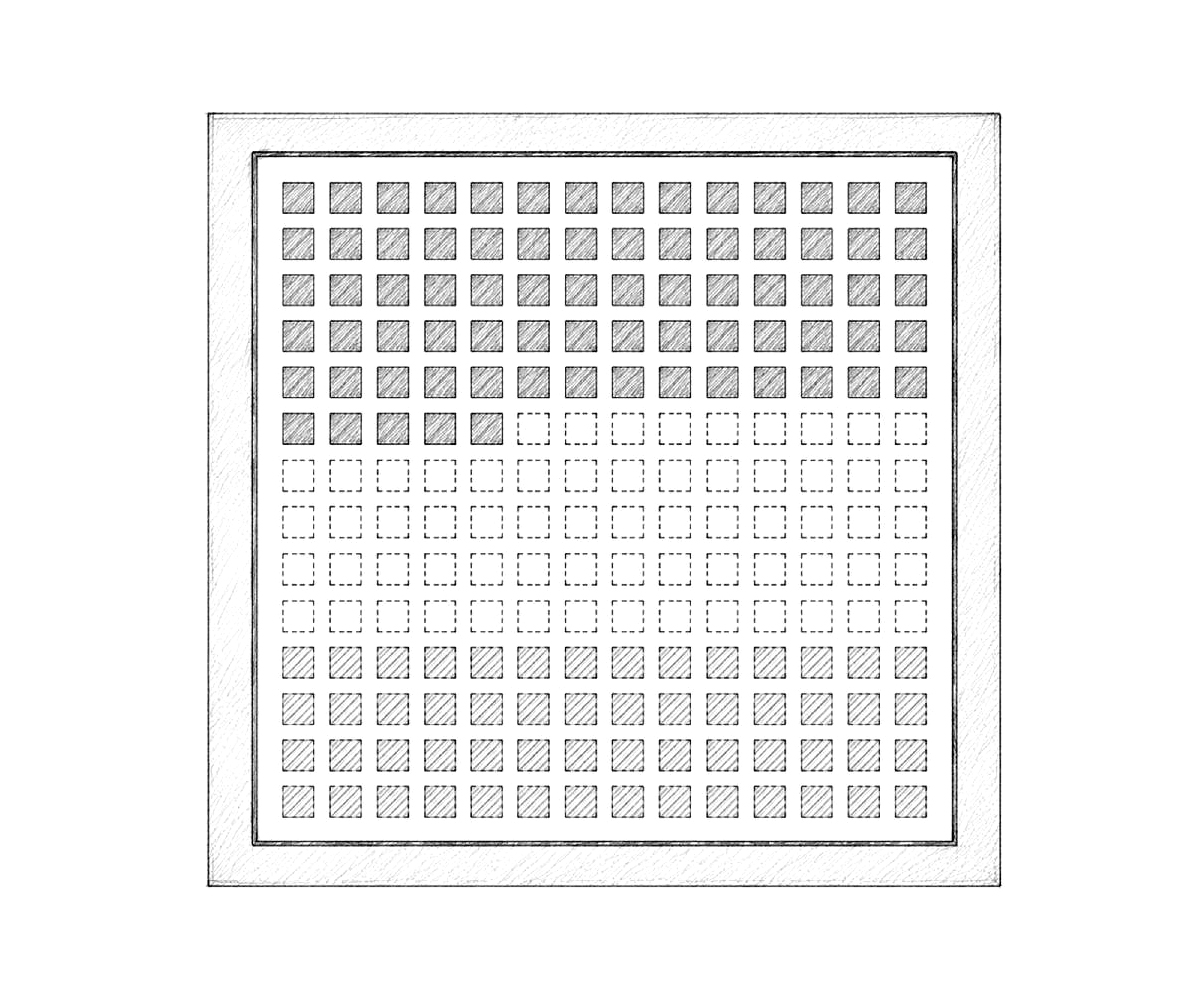
FOPLP Advanced Packaging Applications
FOPLP (Fan-Out Panel Level Packaging) is one of the most significant emerging technologies in advanced semiconductor packaging. Compared with traditional Fan-Out Wafer Level Packaging (FOWLP), FOPLP utilizes large-format panel-based manufacturing processes, significantly increasing production capacity while reducing cost per unit, making it a key technology for future high-performance and cost-effective packaging solutions.
FOPLP offers numerous advantages, including high I/O density, ultra-thin package profiles, improved electrical performance, and high-volume manufacturing capability. It is widely adopted in consumer electronics, AI edge computing, automotive electronics, 5G communications, RF modules, and other advanced semiconductor applications.
At Zhanyang, we provide comprehensive core components, precision tooling, and fixture solutions for FOPLP packaging processes. Leveraging our expertise in semiconductor manufacturing, precision machining, and advanced packaging technologies, we help customers achieve higher yields, improved process stability, and reliable mass production performance.
FOPLP Packaging Process Flow
The FOPLP process mainly consists of the following key steps:
- Die Placement / Reconstitution: Arrange semiconductor dies onto a large-format panel carrier.
- Molding Process: Encapsulate the entire panel using Epoxy Molding Compound (EMC).
- Redistribution Layer (RDL) Formation: Create high-density electrical interconnections.
- Surface Finishing & Plating: Form conductive layers and electrical pathways.
- Singulation / Dicing: Separate the panel into individual packaged devices.
The key to FOPLP manufacturing lies in large-panel process control, high-precision alignment, and high-yield production capability.
FOPLP Process Technical Challenges
- Panel Warpage: Large-size panels are prone to deformation during thermal processes.
- Panel Alignment: Requires micron-level or even higher alignment accuracy.
- RDL Reliability: Fine redistribution traces are susceptible to open circuits and short circuits.
- Package Stress: Material property differences may lead to deformation and cracking.
- Yield Management: As panel size increases, maintaining high production yield becomes more challenging.
As a result, market demand for high-rigidity fixtures, ultra-flat carriers, and precision machining capabilities continues to grow significantly.
Our Core Technical Capabilities
We provide:
● Core fixture design for FOPLP packaging processes
● Development of precision components for panel-level manufacturing
● Large-format, high-precision machining capabilities
Technical Expertise:
● Large-area flatness control technology
● Ceramic and metal composite material machining
● Ultra-precision grinding and polishing
● Micron-level positioning and structural design
Enabling packaging processes with high flatness, superior stability, and exceptional consistency.
Key Product Solutions for FOPLP Packaging
Panel Carrier / Panel Tray
The foundation of a stable FOPLP process.
● High-flatness control
● Anti-warpage design
● High-cleanliness materials
Vacuum Chuck
Ensures stable panel fixation and processing.
● Uniform vacuum distribution across large areas
● High-precision flatness control
Stage / Heating Plate
Controls molding and RDL process temperatures.
● Excellent temperature uniformity
● Large-area thermal control capability
Custom Fixtures
Improve process alignment accuracy and stability.
● Panel positioning fixtures
● Process transfer fixtures
Thermal & Structural Components
Address thermal challenges in high-density packaging.
● High thermal conductivity materials (AlSiC / Copper)
● Low CTE structural designs
Technical Advantages
- Precision machining capabilities for panel-level packaging.
- Advanced large-area flatness control technology.
- Customized FOPLP process solutions.
- Strong support for high-yield mass production.
Applications
- Mobile Devices & Wearables.
- AIoT / Edge AI Applications.
- Automotive Electronics.
- 5G / RF Modules.
- Consumer Electronics.
Why Choose Zhanyang
We provide more than just components—we deliver:
Complete FOPLP Panel-Level Packaging Solutions
Zhanyang focuses on optimizing FOPLP panel-level fan-out packaging processes. Through high-flatness carriers, precision fixtures, and large-panel process control technologies, we effectively address panel warpage and alignment challenges. Our solutions support the future of high-volume, cost-effective advanced packaging, helping customers achieve greater productivity, higher yields, and long-term manufacturing stability.


