

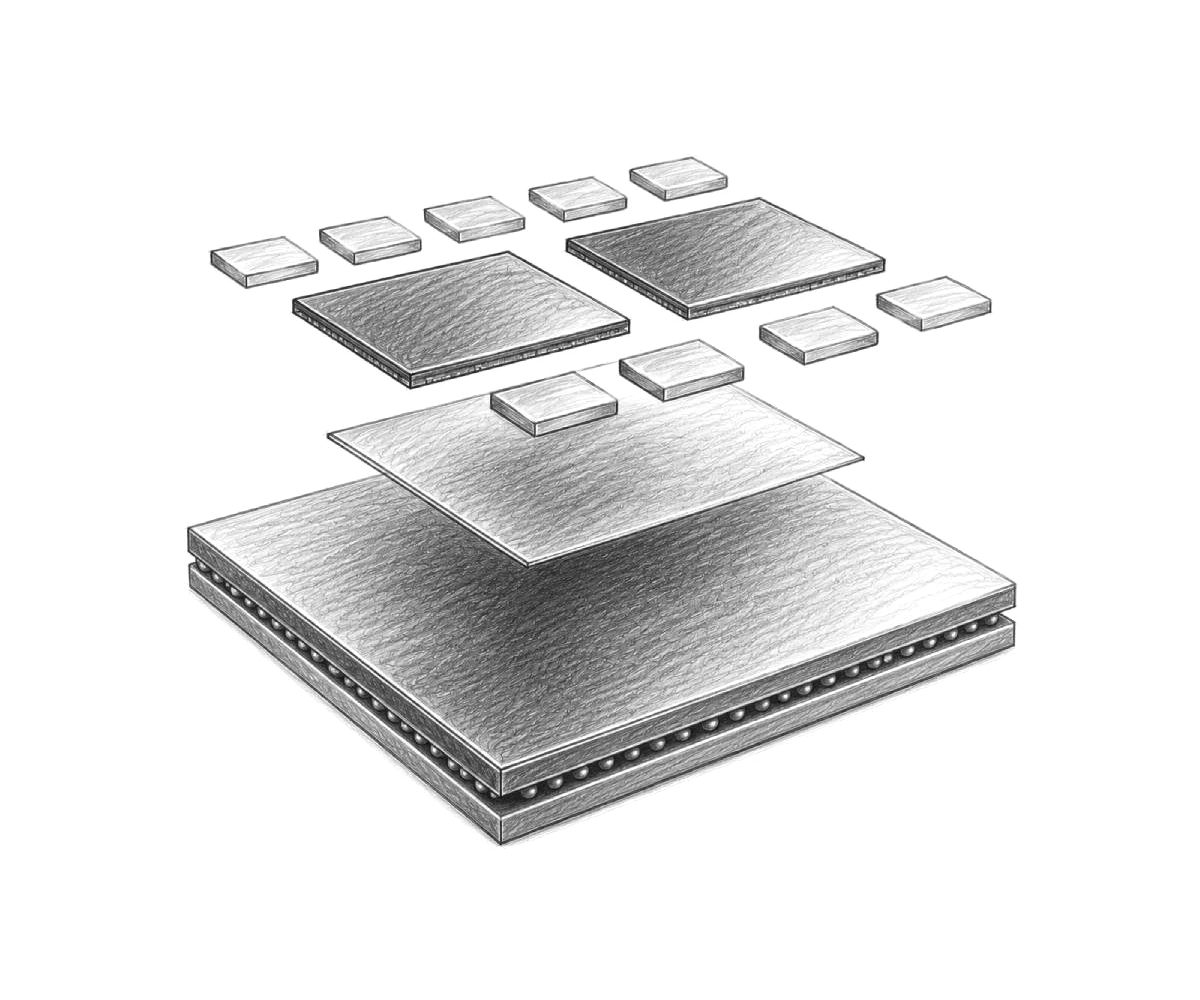
CoWoS Advanced Packaging Applications
CoWoS (Chip-on-Wafer-on-Substrate) technology is one of the most important advanced packaging solutions in today’s semiconductor industry. Utilizing a 2.5D IC integration architecture, CoWoS enables multiple high-performance chips—such as CPUs, GPUs, and HBM (High Bandwidth Memory)—to be integrated on a silicon interposer, achieving ultra-high bandwidth, low-latency communication, and superior system-level performance.
As AI, HPC (High-Performance Computing), and next-generation data center applications continue to drive demand for higher computing power, CoWoS has become a key enabling technology for advanced semiconductor packaging. It provides the performance, power efficiency, and integration density required by modern computing platforms while supporting increasingly complex multi-chip and chiplet-based architectures.
Zhanyang provides a comprehensive portfolio of critical CoWoS packaging components, precision fixtures, and process tooling solutions to support advanced semiconductor manufacturing. Leveraging extensive semiconductor process expertise, precision machining capabilities, and custom engineering services, we help customers improve packaging accuracy, process stability, manufacturing efficiency, and production yield for next-generation high-performance computing devices.
CoWoS Packaging Process Flow
The CoWoS packaging process consists of the following key steps:
Silicon Interposer Fabrication
● TSV (Through Silicon Via) processing
● High-density metal interconnects
Chip-on-Wafer Integration
● Die attachment onto the silicon interposer
● High-precision alignment (Alignment < 5 μm)
Wafer-on-Substrate Assembly
● Bonding the integrated structure onto an organic substrate
Redistribution Layer (RDL) & Encapsulation
● Electrical interconnection and package protection
Testing & Dicing
● Final module testing and singulation
Technical Challenges in CoWoS Packaging
- Large Die Integration: Large chip sizes increase the risk of package warpage
- Thermal Management: High power density generates significant heat
- High-Precision Alignment: Multi-die integration requires extremely precise positioning
- Stress Control: CTE mismatches between different materials can cause deformation
- Yield Control: Complex manufacturing processes create greater yield challenges
- Key Requirements:
● High-precision Bond Tools
● High thermal conductivity materials
● High-rigidity fixtures and tooling
Our Core Technical Capabilities
We provide:
● Development of critical components for CoWoS packaging
● 2.5D packaging process fixture design
● Precision machining and advanced material integration
Technical Capabilities:
● Micron-level precision machining
● High thermal conductivity materials (AlSiC / Copper Alloys)
● Precision ceramic machining (AlN)
● Ultra-precision grinding and flatness control
Delivering: High Precision x Superior Thermal Performance x Exceptional Stability
Key Precision Components and Tooling Support for CoWoS Packaging
In CoWoS-related advanced packaging processes, multi-die bonding, thermal management, pressure control, and wafer handling stability all play important roles in maintaining packaging accuracy and process consistency. Based on customer drawings, equipment interfaces, and process requirements, Zhanyang provides precision component machining and customized tooling support for related CoWoS packaging applications.
Bond Tool
Bond Tools are used in die attach or chip bonding-related processes to support contact surface flatness, thermal stability, and bonding consistency.
● High-flatness machining requirements
● Excellent thermal stability
● Materials such as M390, ceramics, and tungsten carbide can be evaluated based on application requirements
Heating Stage
Heating Stages serve as heating and support platforms during bonding-related processes, helping maintain process temperature, contact stability, and thermal distribution consistency.
● Thermal uniformity support
● Stable process temperature control
● Customizable design based on equipment dimensions and interface requirements
Bonding Head
Bonding Heads are used for pressure transfer and positioning support during bonding or pressing processes, helping improve pressure distribution stability and reduce misalignment risks.
● High-rigidity structure
● Uniform pressure distribution
● Customizable design based on bonding area and equipment requirements
AlSiC Heat Sink
AlSiC Heat Sinks are suitable for high-power chips and high-thermal-density packaging applications, helping improve heat dissipation efficiency and reduce risks related to thermal deformation and CTE mismatch.
● High thermal conductivity
● Low coefficient of thermal expansion (Low CTE)
● Applicable to thermal management structures for advanced packaging-related applications
Wafer Carrier / Custom Fixture
Wafer carriers and customized fixtures are used for wafer or package handling, positioning, support, and process transfer, helping improve process stability and equipment compatibility.
● High-flatness and high-rigidity support
● Helps reduce handling and positioning deviation risks
● Customizable based on wafer size, equipment interface, and process requirements
Technical Advantages
- High-precision 2.5D packaging manufacturing capabilities.
- Advanced thermal management material integration expertise.
- Customized CoWoS packaging solutions.
- Proven long-term mass production stability.
Applications
- AI and GPU processors.
- High-Performance Computing (HPC).
- Data Centers.
- Networking and Communication Equipment.
- High-Speed Computing Platforms.
Why Choose Zhanyang
We provide more than components—we deliver complete CoWoS Advanced Packaging Solutions.
Our expertise focuses on optimizing CoWoS 2.5D advanced packaging processes through high-precision Bond Tools, Heating Stages, and thermal management module design. By effectively addressing challenges associated with high power density and multi-die integration, we help enable the next generation of AI processors and high-performance computing devices.
With extensive experience in semiconductor packaging, precision machining, advanced materials, and thermal management technologies, Zhanyang is your trusted partner for achieving higher packaging yields, improved reliability, and superior manufacturing performance in advanced semiconductor applications.


