

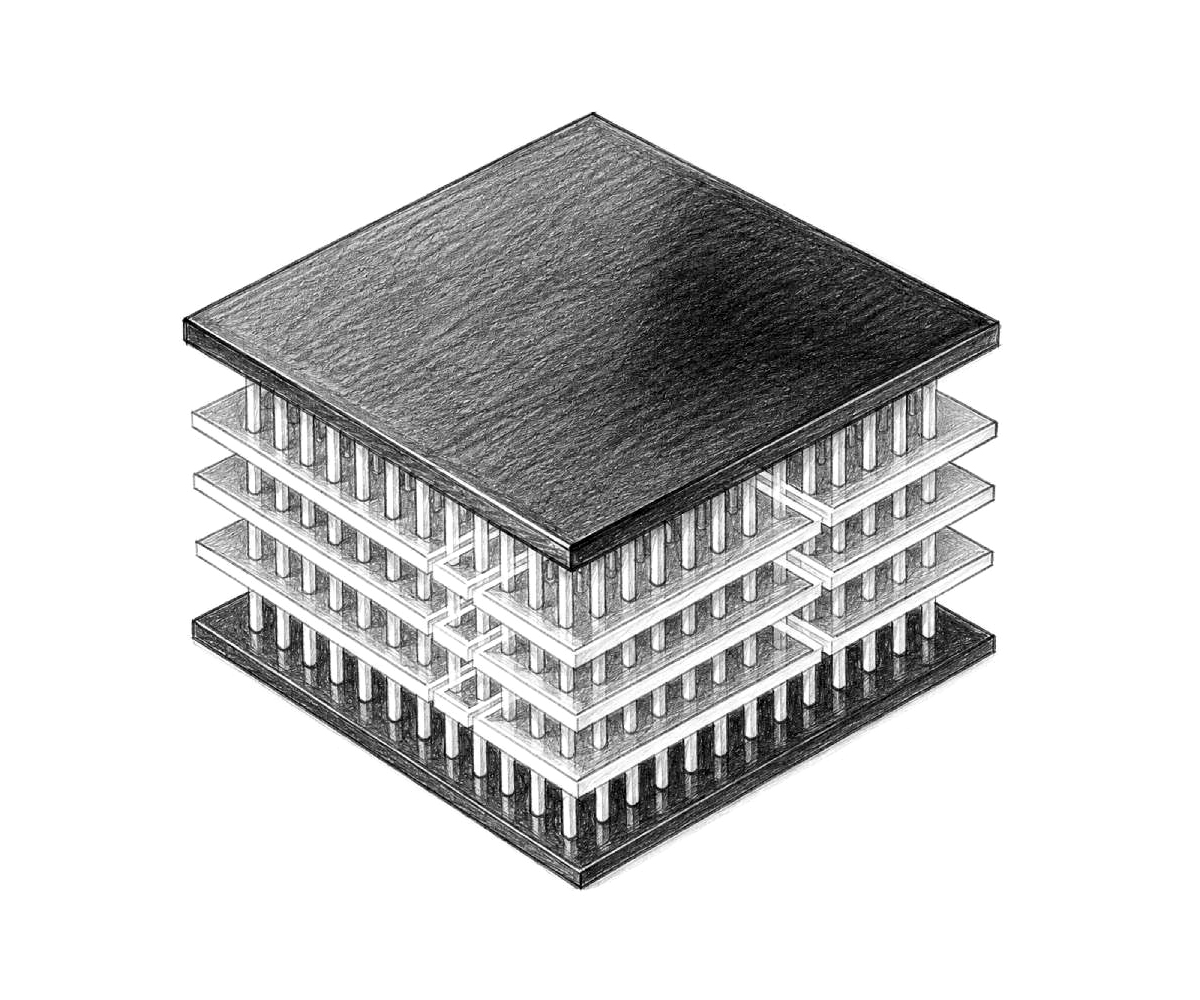
SoIC Advanced Packaging Applications
SoIC (System on Integrated Chips) technology is one of the key innovations in advanced semiconductor packaging. By utilizing Chip-to-Chip (C2C) and Chip-to-Wafer (C2W) 3D stacking technologies, SoIC enables higher performance, lower power consumption, and greater bandwidth through advanced system-level integration.
Compared with conventional packaging technologies, SoIC offers significant advantages, including ultra-high interconnect density, extremely short signal paths, enhanced electrical performance, and superior thermal management capabilities. It is widely adopted in applications such as Artificial Intelligence (AI), High-Performance Computing (HPC), Data Centers, 5G communications, and automotive electronics.
At Zhanyang, we provide comprehensive SoIC packaging process core components and precision fixture solutions to support high-precision 3D stacking manufacturing. Leveraging our expertise in semiconductor processing, precision machining, advanced materials, and packaging integration technologies, we help customers achieve higher alignment accuracy, improved package reliability, enhanced thermal performance, and stable high-volume production for next-generation semiconductor devices.
SoIC Packaging Process Flow
The SoIC process mainly consists of the following key steps:
Wafer Fabrication
● Fabrication of logic and memory devices
Wafer Thinning
● Reduce wafer thickness to less than 50 μm to enable 3D stacking
Alignment & Bonding
● Die-to-Die Bonding
● Die-to-Wafer Bonding
● Alignment accuracy requirement of less than 1 μm (sub-micron level)
Hybrid Bonding
● Combines Cu-to-Cu interconnects with dielectric bonding technology
Back-End Processing
● Final packaging and testing
SoIC Process Technical Challenges
- Sub-Micron Alignment: Alignment errors must be controlled within 1 μm or even nanometer-level tolerances.
- Wafer Warpage: Thin wafers are highly susceptible to deformation during processing.
- CTE Mismatch: Differences in the coefficient of thermal expansion among materials can lead to stress concentration.
- Bonding Voids: Defects at the bonding interface can affect electrical performance and long-term reliability.
- Ultra-Thin Die Handling: Dies thinner than 50 μm are extremely fragile and prone to cracking.
As a result, demand for high-precision Bond Tools, highly stable stages, and precision fixture designs continues to increase significantly.
Our Core Technical Capabilities
We provide:
● Core component design for SoIC packaging processes
● Precision fixture development for 3D IC manufacturing
● High-precision machining and material integration services
Technical Capabilities:
● Micron and sub-micron machining technology
● Precision ceramic machining (AlN / Al₂O₃)
● High thermal conductivity materials (AlSiC)
● Ultra-precision grinding and polishing
Delivering advanced packaging solutions with exceptional precision, stability, and reliability.
Key Product Solutions for SoIC Packaging
Bond Tool
A critical component for SoIC bonding processes.
● Materials: AlN Ceramic / M390 / Tungsten Carbide
● Nanometer-level flatness
● Excellent thermal stability
Ensures hybrid bonding quality and bonding interface reliability.
Heating Stage
Controls bonding temperature and thermal uniformity.
● Superior temperature uniformity
● Rapid heating and cooling response
● High thermal conductivity design
Bonding Head
Provides precise pressure control.
● High-rigidity structure
● Uniform pressure distribution
● Anti-misalignment design
Thin Die Fixture
Prevents damage to ultra-thin dies.
● Optimized vacuum holding design
● Anti-deformation structure
AlSiC Heat Sink
Addresses high power density thermal challenges.
● High thermal conductivity
● Low coefficient of thermal expansion (CTE)
Technical Advantages
- Nano-level precision machining capability.
- Advanced packaging material integration expertise.
- Customized SoIC process solutions.
- High-stability and long-lifetime designs.
Applications
- AI Chips.
- High-Performance Computing (HPC).
- Data Centers.
- 5G Communications.
- Automotive Electronics.
Why Choose Zhanyang
We provide more than just components—we deliver:
Complete SoIC 3D Packaging Solutions
Zhanyang focuses on optimizing SoIC advanced packaging and 3D IC stacking processes. Through high-precision Bond Tools, Heating Stages, and custom fixture designs, we effectively address nanometer-level alignment and bonding stability challenges, providing critical technology support for the next generation of AI and high-performance computing devices.


