

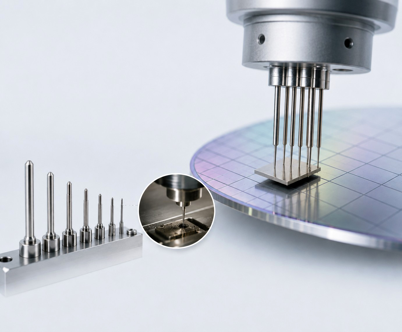
Thin Die Ejector Pin Assembly Optimization Case Study
Targeting a Die Pick Yield Improvement to 99%
In semiconductor packaging processes, particularly in System-in-Package (SiP) and Advanced Packaging applications, the demand for stable handling of small and ultra-thin chips continues to increase. Conventional Ejector Pin Assemblies, typically made of aluminum, can no longer meet the precision and high-yield requirements of Die Bonding processes, often resulting in die cracking, chip drop-off, and reduced pick-up reliability.
Process Pain Points and Engineering Challenges
In high-precision semiconductor packaging processes, Die Bonding requires exceptional positioning accuracy, surface quality, and component stability. However, conventional equipment and components often face significant engineering challenges.
For example, Die Bond pick-up yield is typically around 95%, falling short of advanced packaging requirements. Ultra-thin dies (0.05 mm) are prone to cracking or chipping due to stress concentration during pick-and-place operations. In addition, conventional aluminum ejector pin assemblies often exhibit insufficient flatness (approximately 5 μm), resulting in uneven die support and reduced bonding stability. Excessive surface roughness (Ra 1.6 μm) can also lead to die scratching and positioning errors. Furthermore, inadequate micro-hole precision and roundness (20 μm), combined with oversized ejector pins that cause interference, can negatively impact the handling accuracy of small dies and overall packaging yield, making it difficult to meet the stringent requirements of advanced semiconductor packaging applications.
Solution
To address die pick-up stability and micro-die processing challenges in high-precision semiconductor packaging applications, we implemented a Hybrid Ejector Pin Design utilizing a combination of Tungsten Carbide and Stainless Steel. This hybrid structure significantly improves hardness, wear resistance, and overall mechanical stability while overcoming the strength and precision limitations associated with conventional aluminum designs. The result is reduced deformation and wear during long-term operation.
In addition, through advanced precision grinding technology, the ejector pin assembly achieves a flatness of <2 μm and a surface roughness of Ra <0.65 μm, providing more uniform and stable die support. This design is particularly suitable for 0.05 mm ultra-thin dies and high-yield Die Bond processes, effectively minimizing die cracking and die shift risks.
For micro-machining applications, high-precision micro-hole processing technology was adopted, enabling hole diameters as small as Ø0.21 mm with roundness controlled to <10 μm. Combined with a miniature ejector pin design of SR0.15 mm, the solution supports small die handling, high-density packaging, and advanced semiconductor manufacturing requirements, further improving pick-up accuracy and packaging yield.
Process Validation
● Test Site: Leading Semiconductor Packaging Company in Taiwan
● Test Condition: 40,000 Die Pick & Place Cycles
● Application: Thin Die Handling Process
Test Results
● Target Achieved: Die Pick Yield Improved to Over 99% (High-Yield Semiconductor Process).
● Significant Reduction in Die Cracking.
● Enhanced Die Bond Process Stability.
Customer Benefits
Cost and Lead Time Reduction
● Target: 25% Cost Reduction
● Target: 50% Shorter Lead Time
Enhanced Packaging Competitiveness
● Supports SiP, 2.5D, and 3D Packaging Technologies
● Suitable for AI, Automotive, and IoT Chips
Localization of Critical Components
● Reduced Dependence on Imported Components
● Improved Supply Chain Stability
Case Study Summary
This project successfully addressed thin-die pick-up yield challenges through an advanced Ejector Pin Design and Precision Micro-Machining Technology, achieving an optimized solution with high yield (>99%) and lower overall manufacturing costs.
Leveraging its expertise in precision machining, multi-material integration, and advanced packaging processes, Zhanyang continues to help customers overcome technical challenges associated with ultra-thin dies and high-density packaging applications, establishing itself as a trusted technology partner in advanced semiconductor packaging and precision component manufacturing.


